
Rocket flight controller V1
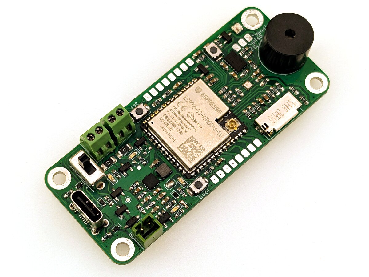 This is my attempt at making a fully integrated flight controller for a model rocket. My previous attempts at avionics were using modules wired together, which was too limiting, heavy and unreliable. I decided to use an ESP32 MCU for this project, because I have the most experience with it and I didn't want to increase the scope even further by learning about a new MCU. The bluetooth capability might also come in handy for pre-flight telemetry. This is my first "real" project in KiCAD and I have made a couple of mistake, so don't follow this as a guide.
The requirements for this project are based mainly on my experience with rocket avionics:
- MCU:
- ESP32 MCU
- Boot button
- Reset button
- USB-C connector capable of flashing the MCU
- Sensors:
- High g accelerometer (>100g)
- Barometer capable of determining apogee
- Battery voltage sensor
- Logging:
- SD card slot
- Separate SPI lane for the SD card and the sensors
- Human interface:
- Control button
- NeoPixel LED
- Buzzer
- Power management:
- 1s lithium battery input
- USB-C power input
- Automatic power input switching
- 1s lithium battery charger
- Power switch
- 3V3 buck boost regulator
- Switchable 3V3 rail for peripherals (anything apart from the ESP32)
- Ejection charge:
- 2 outputs
- Screw in terminals
- LED signalization for the output state
- Possibility for a switch in series for a remove before flight pin
- Structural:
- 4 M3 mounting holes
- Dimensions as small as possible
MCU
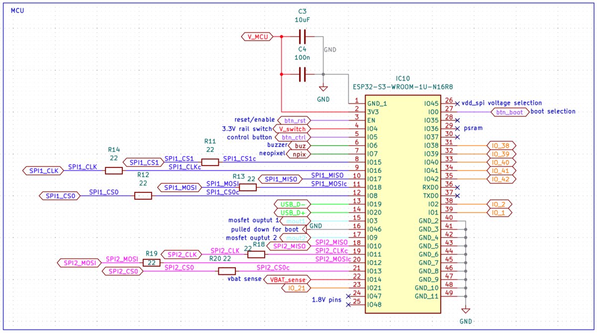
I decided to use the ESP32-S3-WROOM-1U-N16R8 for several reasons. The wroom module includes the MCU, oscillator and memory, so it saves me some work and I can be sure it is going to work. The 1U version comes without the integrated antenna, which makes it a little bit smaller and you don't have to place it on the edge of the PCB. The S3 can be directly programmed from a USB, so you don't have to use a USB to UART bridge.
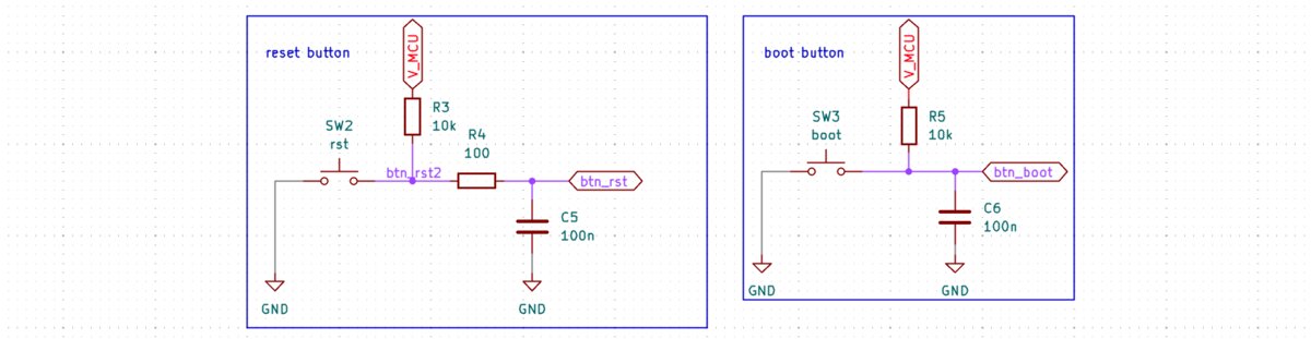
The boot and reset buttons are wired accordingly to the official documentation.
Sensors
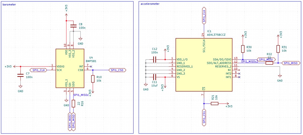
I decided to go with the ADXL375BCCZ accelerometer, because it is one of the few ones that measure acceleration higher than 100g. The barometer is BMP581, because it has a high accuracy and is rather cheap. For the battery voltage sensor I used a simple voltage divider and an ADC input on the ESP32.
Logging
For the SD card connector, I chose one that allows the SD card to rest above the components on the PCB, which saves a lot of space. The SD card uses its own SPI lane as per requirements.

Human interface
The flight controller communicates with a human in 3 ways. The input is a simple button meant for switching the program states. The output is a single NeoPixel LED and an active buzzer. It is turned on and off by a P-channel mosfet in order to not overload the ESP32 IO pin.

Ejection charge outputs
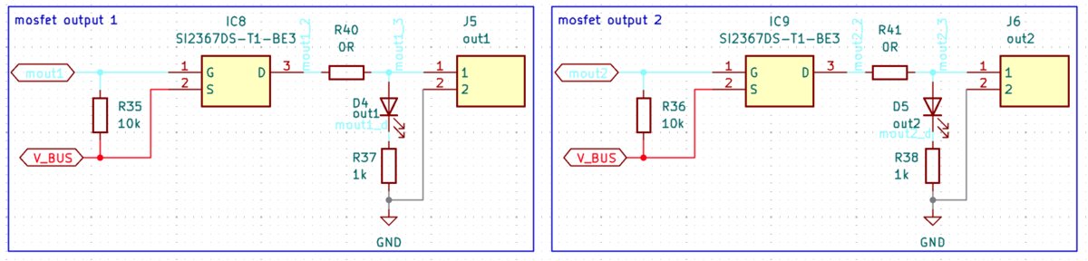
The flight controller has 2 ejection charge outputs to allow for staging or multi-stage parachutes. The ejection charges are connected using small screw in terminals. Each output uses a P-channel mosfet as a switch in order to not overload the IO pins. The input voltage is from the main power rail (USB or battery). This is done to bypass the 3V3 regulator in order to not overload it during firing. There is a 0 ohm 1206 resistor between the mosfet and the terminal. This resistor can be removed, which reveals 2 solder pads on which a remove before flight switch can be soldered. Each output has an LED wired to it. This is a safety mechanism, which warns you to not plug in the ejection charge when the LED is shining.
Power management
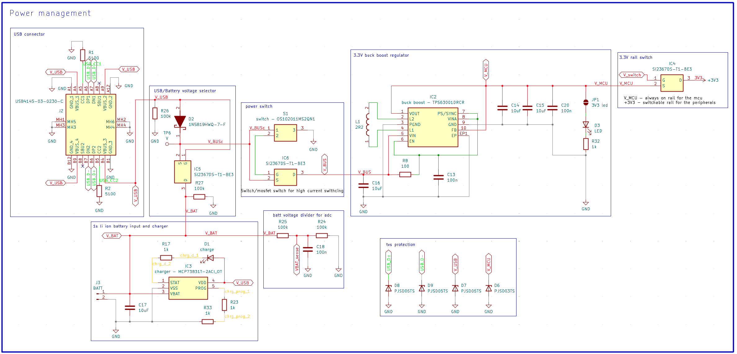
This is the whole power management schematic (click on the image to enlarge it):
USB-C connector
I had to use a right angle USB-C cable in the past in order to connect to the avionics with a horizontal connector. For that reason this flight controller has a vertical USB-C connector. This makes it easier to plug in the cable while the flight controller is mounted in the rocket.
The CC pins of the USB are pulled down as per the USB documentation.
Voltage selector
The voltage selector chooses the input to the main voltage rail in between the USB-C and battery while prioritizing the USB. The circuit is taken from this Microchip article.
Battery input and charger
The input for the battery is via a 2 pin JST PH-K commonly found on small lithium batteries. Charging is handled using the MCP73831. The circuit around the charger is taken from the datasheet.
Power switch
Most small switches are rated for tiny currents (100-300mA). This might not be enough for this flight controller, so I chose to use a P-channel mosfet as a switch operated by the physical switch.
Buck boost regulator
At first I wanted to use an LDO to regulate the voltage. The issue with an LDO would be the voltage range (2.7-4.1V) of a 1s li-ion battery. Even a good LDO would stop working at around 3.4V, which would leave around 50% of the battery capacity unused. For that reason I decided to go with a buck boost regulator, which can handle the whole voltage range of the battery. The disadvantage is the increased complexity and increased noise.
3V3 rail switch
The main point of the 3V3 rail switch is a battery undervoltage protection. The idea is that the ESP32 constantly monitors the battery voltage using the voltage divider and when it reaches a low value, it turns off the power to all the peripherals and goes to deep sleep. This drastically lowers the power consumption and stops draining the battery.
PCB design
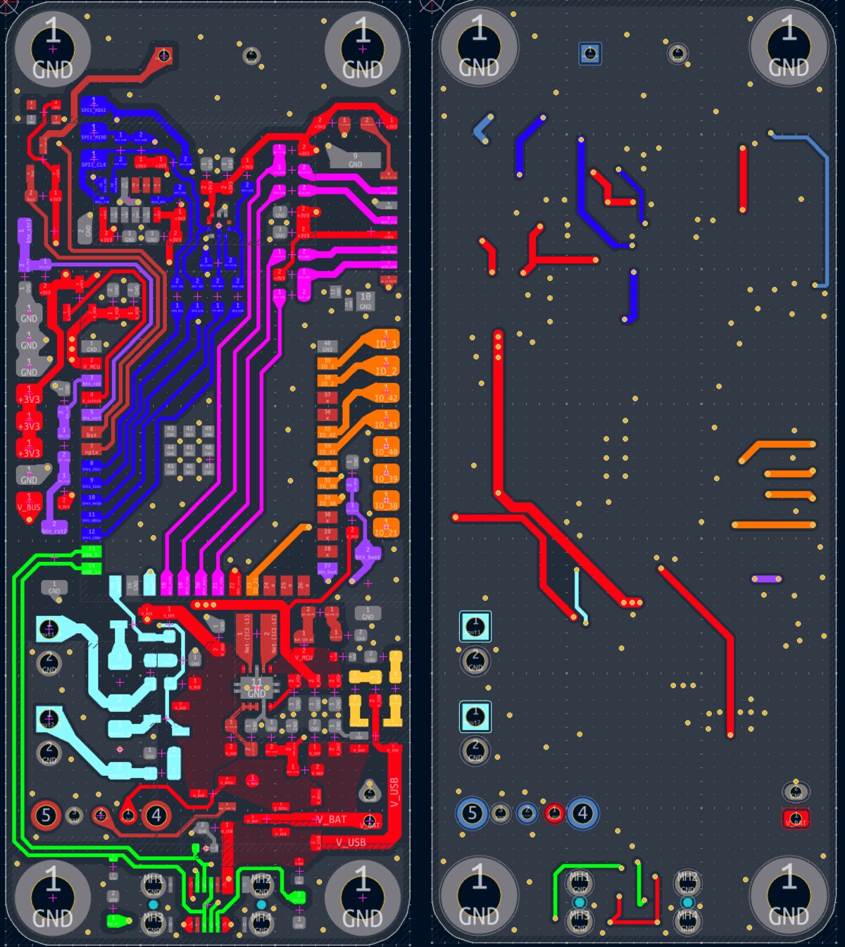
The flight controller has rectangular shape of 30x70mm. This makes it fit into rockets with a small diameter. The PCB is split into 3 regions. The top one houses the sensors, SD card and the human interface components. The middle one is the MCU with its buttons. The bottom one is for power management, ejection charge outputs and connectors. All the components are only on one side to make the soldering easier. I tried to fit all of it on a 2 layer PCB to reduce the cost. This was a challenge, but I managed to do it and ended up with a decent ground plane. The USB traces are routed on the edge of the PCB to move them far away from the noisy buck boost converter.
Assembly
I ordered the PCBs on JLCPCB. It only cost about 20 USD for 5 of them with the express shipping. I did not get a solder stencil, because It thought I could do it without it.
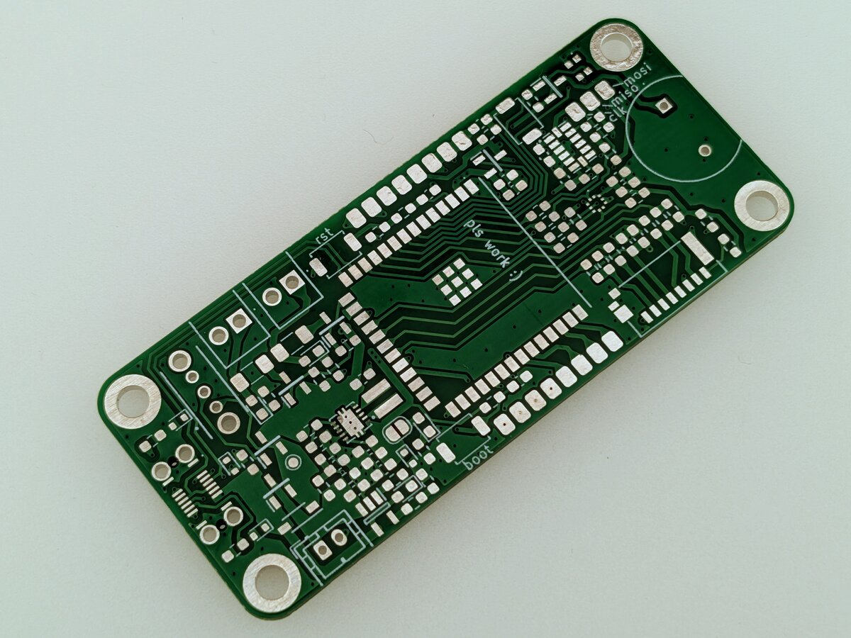 The accelerometer, barometer, SD card connector, buck boost converter, inductor and the ESP32 were soldered using solder paste and a hot plate. I did the rest by hand with a soldering iron. This took a full day and the result was not very good. Next time I am going to get the stencil.
Issues
This is the list of known issues so far that need to be fixed in the next version.
Ejection charge outputs
The ejection charge outputs don't work properly. I am using P-channel mosfets to switch the outputs, which require negative gate to source voltage to be closed and positive to be open. I added a pull up resistor to the output to keep them open when the IO pin is floating. This pull up back feeds up to 5V to the ESP32, which is higher than it is rated for. Removing the pull up doesn't solve this issue, because the ESP32 itself cannot supply the required voltage to keep the mosfet open.
There are couple solutions, but I am not sure which one I want to use. The first one is to use an N-channel mosfet for low side switching. This solution seems less safe as there will always be voltage going to the ejection charges. It also adds additional component to the BOM.
The other solution is to use a gate driver to drive the mosfets. This solution adds more components to the PCB and increases complexity and cost.
3V3 rail
The voltage on the 3V3 rail is 3V7. This is above the absolute maximum of some of the components it powers. I am not sure why, and I need to investigate it more. The buck boost converter I am using is fixed at 3V3, so it cannot be an improper voltage setting.
Improvements
These are some improvements that would be nice to implement in the next version:
- The human interface components on top are not easily accessible in my use case. It would be better to have them at the bottom.
- Add an IMU for high accuracy acceleration and rate of rotation.
- Remove some unnecessary resistors, test points, jumpers, etc. to save some space.
- Use 0402 resistors instead of 0603 to save more space.
- Use a smaller power switch.
- Add a physical debounce to the power switch to prevent power loss due to vibrations.
- Use larger resistor values for the LEDs.
- The buzzer might not need a mosfet for switching.